- 您现在的位置:买卖IC网 > Sheet目录3826 > PIC18F4455-I/ML (Microchip Technology)IC PIC MCU FLASH 12KX16 44QFN
PIC18F2455/2550/4455/4550
DS39632E-page 138
2009 Microchip Technology Inc.
13.2
Timer2 Interrupt
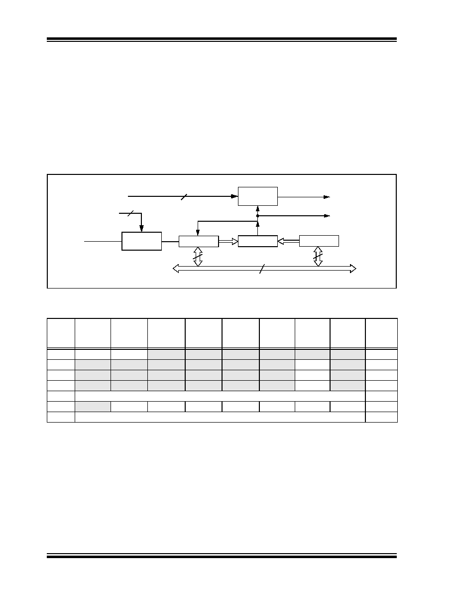
Timer2 can also generate an optional device interrupt.
The Timer2 output signal (TMR2 to PR2 match) pro-
vides the input for the 4-bit output counter/postscaler.
This counter generates the TMR2 match interrupt flag
which is latched in TMR2IF (PIR1<1>). The interrupt is
enabled by setting the TMR2 Match Interrupt Enable
bit, TMR2IE (PIE1<1>).
A range of 16 postscale options (from 1:1 through 1:16
inclusive) can be selected with the postscaler control
bits, T2OUTPS3:T2OUTPS0 (T2CON<6:3>).
13.3
TMR2 Output
The unscaled output of TMR2 is available primarily to
the CCP modules, where it is used as a time base for
operations in PWM mode.
Timer2 can be optionally used as the shift clock source
for the MSSP module operating in SPI mode.
Additional information is provided in Section 19.0
FIGURE 13-1:
TIMER2 BLOCK DIAGRAM
TABLE 13-1:
REGISTERS ASSOCIATED WITH TIMER2 AS A TIMER/COUNTER
Comparator
TMR2 Output
TMR2
Postscaler
Prescaler
PR2
2
FOSC/4
1:1 to 1:16
1:1, 1:4, 1:16
4
T2OUTPS3:T2OUTPS0
T2CKPS1:T2CKPS0
Set TMR2IF
Internal Data Bus
8
Reset
TMR2/PR2
8
(to PWM or MSSP)
Match
Name
Bit 7
Bit 6
Bit 5
Bit 4
Bit 3
Bit 2
Bit 1
Bit 0
Reset
Values
on page
INTCON GIE/GIEH PEIE/GIEL
TMR0IE
INT0IE
RBIE
TMR0IF
INT0IF
RBIF
PIR1
SPPIF(1)
ADIF
RCIF
TXIF
SSPIF
CCP1IF
TMR2IF
TMR1IF
PIE1
SPPIE(1)
ADIE
RCIE
TXIE
SSPIE
CCP1IE
TMR2IE
TMR1IE
IPR1
SPPIP(1)
ADIP
RCIP
TXIP
SSPIP
CCP1IP
TMR2IP
TMR1IP
TMR2
Timer2 Register
T2CON
—
T2OUTPS3 T2OUTPS2 T2OUTPS1 T2OUTPS0 TMR2ON T2CKPS1 T2CKPS0
PR2
Timer2 Period Register
Legend: — = unimplemented, read as ‘0’. Shaded cells are not used by the Timer2 module.
Note 1: These bits are unimplemented on 28-pin devices; always maintain these bits clear.
发布紧急采购,3分钟左右您将得到回复。
相关PDF资料
PIC24FJ64GB108-I/PT
IC PIC MCU FLASH 80TQFP
DSPIC33FJ64MC506A-I/PT
IC DSPIC MCU/DSP 64K 64-TQFP
PIC16F877A-I/P
IC MCU FLASH 8KX14 EE 40DIP
MP2-HS240-51
CONN SHROUD 2-FB 240POS 5ROW
DSPIC33FJ64MC506-I/PT
IC DSPIC MCU/DSP 64K 64TQFP
DSPIC33FJ128MC802-I/SO
IC DSPIC MCU/DSP 128K 28SOIC
PIC18LF4331-I/P
IC PIC MCU FLASH 4KX16 40DIP
DSPIC33FJ128GP306-I/PT
IC DSPIC MCU/DSP 128K 64TQFP
相关代理商/技术参数
PIC18F4455-I/P
功能描述:8位微控制器 -MCU 24kBF 2048RM FSUSB2 RoHS:否 制造商:Silicon Labs 核心:8051 处理器系列:C8051F39x 数据总线宽度:8 bit 最大时钟频率:50 MHz 程序存储器大小:16 KB 数据 RAM 大小:1 KB 片上 ADC:Yes 工作电源电压:1.8 V to 3.6 V 工作温度范围:- 40 C to + 105 C 封装 / 箱体:QFN-20 安装风格:SMD/SMT
PIC18F4455-I/PT
功能描述:8位微控制器 -MCU 24kBF 2048RM FSUSB2 RoHS:否 制造商:Silicon Labs 核心:8051 处理器系列:C8051F39x 数据总线宽度:8 bit 最大时钟频率:50 MHz 程序存储器大小:16 KB 数据 RAM 大小:1 KB 片上 ADC:Yes 工作电源电压:1.8 V to 3.6 V 工作温度范围:- 40 C to + 105 C 封装 / 箱体:QFN-20 安装风格:SMD/SMT
PIC18F4455T-I/ML
功能描述:8位微控制器 -MCU 24kBF 2048RM FSUSB2 RoHS:否 制造商:Silicon Labs 核心:8051 处理器系列:C8051F39x 数据总线宽度:8 bit 最大时钟频率:50 MHz 程序存储器大小:16 KB 数据 RAM 大小:1 KB 片上 ADC:Yes 工作电源电压:1.8 V to 3.6 V 工作温度范围:- 40 C to + 105 C 封装 / 箱体:QFN-20 安装风格:SMD/SMT
PIC18F4455T-I/PT
功能描述:8位微控制器 -MCU 24kBF 2048RM FSUSB2 RoHS:否 制造商:Silicon Labs 核心:8051 处理器系列:C8051F39x 数据总线宽度:8 bit 最大时钟频率:50 MHz 程序存储器大小:16 KB 数据 RAM 大小:1 KB 片上 ADC:Yes 工作电源电压:1.8 V to 3.6 V 工作温度范围:- 40 C to + 105 C 封装 / 箱体:QFN-20 安装风格:SMD/SMT
PIC18F4458-I/ML
功能描述:8位微控制器 -MCU 24KB Flash 2KB RAM RoHS:否 制造商:Silicon Labs 核心:8051 处理器系列:C8051F39x 数据总线宽度:8 bit 最大时钟频率:50 MHz 程序存储器大小:16 KB 数据 RAM 大小:1 KB 片上 ADC:Yes 工作电源电压:1.8 V to 3.6 V 工作温度范围:- 40 C to + 105 C 封装 / 箱体:QFN-20 安装风格:SMD/SMT
PIC18F4458-I/P
功能描述:8位微控制器 -MCU 24KB Flash 2KB RAM RoHS:否 制造商:Silicon Labs 核心:8051 处理器系列:C8051F39x 数据总线宽度:8 bit 最大时钟频率:50 MHz 程序存储器大小:16 KB 数据 RAM 大小:1 KB 片上 ADC:Yes 工作电源电压:1.8 V to 3.6 V 工作温度范围:- 40 C to + 105 C 封装 / 箱体:QFN-20 安装风格:SMD/SMT
PIC18F4458-I/PT
功能描述:8位微控制器 -MCU 24KB Flash 2KB RAM RoHS:否 制造商:Silicon Labs 核心:8051 处理器系列:C8051F39x 数据总线宽度:8 bit 最大时钟频率:50 MHz 程序存储器大小:16 KB 数据 RAM 大小:1 KB 片上 ADC:Yes 工作电源电压:1.8 V to 3.6 V 工作温度范围:- 40 C to + 105 C 封装 / 箱体:QFN-20 安装风格:SMD/SMT
PIC18F4458T-I/ML
功能描述:8位微控制器 -MCU 24KB Flash 2KB RAM RoHS:否 制造商:Silicon Labs 核心:8051 处理器系列:C8051F39x 数据总线宽度:8 bit 最大时钟频率:50 MHz 程序存储器大小:16 KB 数据 RAM 大小:1 KB 片上 ADC:Yes 工作电源电压:1.8 V to 3.6 V 工作温度范围:- 40 C to + 105 C 封装 / 箱体:QFN-20 安装风格:SMD/SMT